The Reason for the Leakage Current of MOS Tube

0:09 / 14:20 Measuring the leakage current of a MOSFET
The cause of the MOS tube's leakage current
Power dissipation is caused by leakage current, especially at lower threshold voltages. Learn about the six different causes of leakage currents in MOS transistors.
1. Reverse bias - leakage current at the PN junction
2. Leakage current below the threshold
3. Reduction of the barrier due to drainage
4. Vth roll-off
5. The impact of the working environment's temperature
6. Leakage current tunneling into and through gate oxide
7. Current leakage from the substrate to the gate oxide layer due to hot carrier injection
8. Current leakage owing to drain decrease generated by the gate (GIDL)
Before continuing, make sure you understand the fundamental concepts of MOS transistors, as this will help you understand what follows.
1. Reverse Biased pn Junction Leakage Current
During transistor operation, MOS transistor s' drain/source and substrate junctions are reverse biased. As a result, the device's leakage current is reverse biased. This leakage current could be caused by minority carrier drift/diffusion in the reverse biased region, as well as the avalanche effect's creation of electron-hole pairs. The reverse bias leakage current at a pn junction is determined by the doping concentration and junction area.
The band-to-band tunneling (BTBT) effect dominates the reverse bias leakage current in strongly doped pn junctions in the drain/source and substrate regions. Electrons tunnel straight from the p-valence region's band to the n-conduction region's band in interband tunneling. For electric fields greater than 10 6 V/cm, BTBT is evident.

Figure 1. Band-to-Band Tunneling in a Reverse-Biased PN Junction of a MOS Transistor
It's worth noting that in the context of this research, we define tunneling as occurring even when the electron's energy is substantially lower than the barrier.
2. Subthreshold leakage current
The transistor is considered to be biased in the subthreshold or weak inversion zone when the gate voltage is less than the threshold value (V th) but larger than zero. The concentration of minority carriers is small, but not zero, in weak inversion. The entire voltage drop occurs at the drain-substrate pn junction in this scenario for |VDS| typical values > 0.1V.
The electric field component parallel to the Si-SiO contact between drain and source is minimal. The drift current is low because to the small electric field, and the subthreshold current is mostly diffusion current.
Drainage Induced Barrier Lowering (DIBL)
Drain induced barrier lowering, or DIBL, is the primary cause of subthreshold leakage current. The depletion zones of the drain and source interact in short-channel devices to lower the source barrier. Subthreshold leakage currents originate from the source injecting charge carriers into the channel surface.
DIBL is evident in high drain voltage and short channel devices.
V th roll off
The threshold voltage of MOS devices falls as channel length decreases. V th roll-off is the name given to this phenomena (or threshold voltage roll-off). The drain and source depletion areas in short-channel devices extend further into the channel length, draining a portion of the channel.
As a result, inverting the channel requires a lower gate voltage, lowering the threshold voltage. This effect is more noticeable at higher drain voltages. Because subthreshold current is inversely related to threshold voltage, lowering the threshold voltage increases subthreshold leakage current.
The effect of operating temperature
Leakage current is also affected by temperature. The threshold voltage falls as the temperature rises. In other words, as the temperature rises, the subthreshold current rises as well.
3. Tunneling into and through the gate oxide leakage current
Thin gate oxides provide large electric fields on the SiO layer in short-channel devices. Electrons tunnel from the substrate to the gate and from the gate through the gate oxide to the substrate when the oxide thickness is low and the electric field is high, resulting in gate oxide tunneling current.
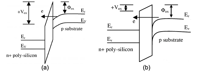
Consider the band diagram shown in the figure.

Figure 2. Band Diagram of a MOS Transistor with (a) Flat Band, (b) Positive Gate Voltage, and (c) Negative Gate Voltage
The first figure, Figure 2(a), is a flat-band MOS transistor. i.e. no charge exists in it.
The band diagram changes when the gate terminal is forward biased, as illustrated in the second graph, Figure 2. (b). Gate current is generated when electrons at the strongly inverted surface tunnel into or through the SiO layer.
A negative gate voltage, on the other hand, causes electrons from the n+ polysilicon gate to tunnel into or through the SiO2 layer, producing in a gate current, as shown in Fig. 2. (c).
Fowler-Nordheim tunnel and direct tunnel
There are mainly two tunneling mechanisms between the gate and the substrate. they are:
Fowler-Nordheim tunneling, where electrons tunnel through a triangular barrier
Direct tunneling, where electrons tunnel through a ladder barrier

Figure 3. Band Diagrams Showing (a) Fowler-Nordheim Tunneling through a Triangular Barrier of Oxides and (b) a Ladder Barrier for Direct Tunneling through Oxides
You can see the band diagrams of the two tunneling mechanisms in Figures 3(a) and 3(b) above.
4. Leakage current due to hot carrier injection from the substrate to the gate oxide
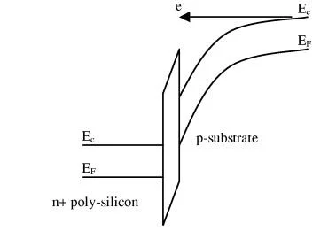
The high electric field near the substrate-oxide interface excites electrons or holes, which pass the substrate-oxide interface and into the oxide layer in short-channel devices. Hot carrier injection is the term for this phenomenon.

Figure 4. Band Diagram Depicting Electrons Gaining Sufficient Energy due to High Electric Field to Cross the Oxide Barrier (Hot Carrier Injection Effect)
Electrons are more susceptible to this phenomena than holes. This is due to the fact that electrons have a lower effective mass and a lower barrier height than holes.
5. Leakage current due to gate induced drain drop (GIDL)
Take an NMOS transistor with a p-type substrate as an example. Positive charge builds exclusively at the oxide-substrate interface when there is a negative voltage at the gate terminal. Due to the holes accumulating on the substrate, the surface behaves as a more strongly doped p-region than the substrate.
As a result, the depletion zone along the drain-substrate contact is thinner near the surface (compared to the thickness of the depletion region in the bulk).

Figure 5. (a) Formation of a Thin Depletion Region Along the Surface at the Drain-Substrate Interface and (b) GIDL Current Flow due to Avalanche Effect and BTBT-Generated Carriers
Avalanche and interband tunneling effects (as discussed in the first part of this study) occur due to the thin depletion area and greater electric field. As a result, minority carriers are created in the drain region under the gate, and the negative gate voltage pushes them into the substrate. Leakage current rises as a result of this.
6. Leakage current due to punch-through effect
Because the drain and source are close together in short-channel devices, the depletion areas of the two terminals converge and eventually overlap. "Penetration" is said to have occurred in this case.
For most carriers from the source, the punch-through effect lowers the barrier. The number of carriers entering the substrate increases as a result of this. The drain collects some of these carriers, while the remainder generate leakage current.
1. How many types of leakage current are there?
There are four types of leakage current:
1. Semiconductor component leakage current
2. Power leakage current
3. Capacitor leakage current
4. Filter leakage current
2. What is the cause of excessive leakage current?
One of the reasons for the excessive leakage current may be caused by a problem with the process of the chip. Generally, the leakage current of the chip will increase when it is used for a long time. For example, the common mobile phone standby time is not long, because the leakage current of the chip is too large. caused.
3. How does temperature affect the leakage current of a MOSFET?
The temperature rise will make the leakage current of the MOSFET smaller, which is the most important characteristic of the MOSFET.
 Discovering New and Advanced Methodology for Determining the Dynamic Characterization of Wide Bandgap DevicesSaumitra Jagdale15 March 20242471
For a long era, silicon has stood out as the primary material for fabricating electronic devices due to its affordability, moderate efficiency, and performance capabilities. Despite its widespread use, silicon faces several limitations that render it unsuitable for applications involving high power and elevated temperatures. As technological advancements continue and the industry demands enhanced efficiency from devices, these limitations become increasingly vivid. In the quest for electronic devices that are more potent, efficient, and compact, wide bandgap materials are emerging as a dominant player. Their superiority over silicon in crucial aspects such as efficiency, higher junction temperatures, power density, thinner drift regions, and faster switching speeds positions them as the preferred materials for the future of power electronics.
Read More A Comprehensive Guide to FPGA Development BoardsUTMEL11 September 202514702
This comprehensive guide will take you on a journey through the fascinating world of FPGA development boards. We’ll explore what they are, how they differ from microcontrollers, and most importantly, how to choose the perfect board for your needs. Whether you’re a seasoned engineer or a curious hobbyist, prepare to unlock new possibilities in hardware design and accelerate your projects. We’ll cover everything from budget-friendly options to specialized boards for image processing, delve into popular learning paths, and even provide insights into essential software like Vivado. By the end of this article, you’ll have a clear roadmap to navigate the FPGA landscape and make informed decisions for your next groundbreaking endeavor.
Read More Applications of FPGAs in Artificial Intelligence: A Comprehensive GuideUTMEL29 August 20253609
This comprehensive guide explores FPGAs as powerful AI accelerators that offer distinct advantages over traditional GPUs and CPUs. FPGAs provide reconfigurable hardware that can be customized for specific AI workloads, delivering superior energy efficiency, ultra-low latency, and deterministic performance—particularly valuable for edge AI applications. While GPUs excel at parallel processing for training, FPGAs shine in inference tasks through their adaptability and power optimization. The document covers practical implementation challenges, including development complexity and resource constraints, while highlighting solutions like High-Level Synthesis tools and vendor-specific AI development suites from Intel and AMD/Xilinx. Real-world applications span telecommunications, healthcare, autonomous vehicles, and financial services, demonstrating FPGAs' versatility in mission-critical systems requiring real-time processing and minimal power consumption.
Read More 800G Optical Transceivers: The Guide for AI Data CentersUTMEL24 December 20253842
The complete guide to 800G Optical Transceiver standards (QSFP-DD vs. OSFP). Overcome supply shortages and scale your AI data center with Utmel Electronic.
Read More Xilinx FPGAs: From Getting Started to Advanced Application DevelopmentUTMEL09 September 20254299
This guide is your comprehensive roadmap to understanding and mastering the world of Xilinx FPGA technology. From selecting your first board to deploying advanced AI applications, we'll cover everything you need to know to unlock the potential of these remarkable devices. The global FPGA market is on a significant growth trajectory, expected to expand from USD 8.37 billion in 2025 to USD 17.53 billion by 2035. This surge is fueled by the relentless demand for high-performance, adaptable computing in everything from 5G networks and data centers to autonomous vehicles and the Internet of Things (IoT). This guide will walk you through the key concepts, tools, and products in the Xilinx ecosystem, ensuring you're well-equipped to be a part of this technological revolution.
Read More
Subscribe to Utmel !
![ATAES132A-MAHER-T]() ATAES132A-MAHER-T
ATAES132A-MAHER-TMicrochip Technology
![TLE8263EXUMA1]() TLE8263EXUMA1
TLE8263EXUMA1Infineon Technologies
![HCS365/P]() HCS365/P
HCS365/PMicrochip Technology
![HCS200/P]() HCS200/P
HCS200/PMicrochip Technology
![DLPA2005ERSLR]() DLPA2005ERSLR
DLPA2005ERSLRTexas Instruments
![ATSHA204-SH-CZ-T]() ATSHA204-SH-CZ-T
ATSHA204-SH-CZ-TMicrochip Technology
![SN74AVC6T622PWR]() SN74AVC6T622PWR
SN74AVC6T622PWRTexas Instruments
![MOC3061VM]() MOC3061VM
MOC3061VMON Semiconductor
![PAM8904JPR]() PAM8904JPR
PAM8904JPRDiodes Incorporated
![AD9961BCPZRL]() AD9961BCPZRL
AD9961BCPZRLAnalog Devices Inc.


 Product
 Brand
Brand Articles
 Tools
Tools


